Fujitsu Develops AI for Image Inspection to Detect Abnormalities in Product Appearance With World-Leading Precision in Key Benchmark
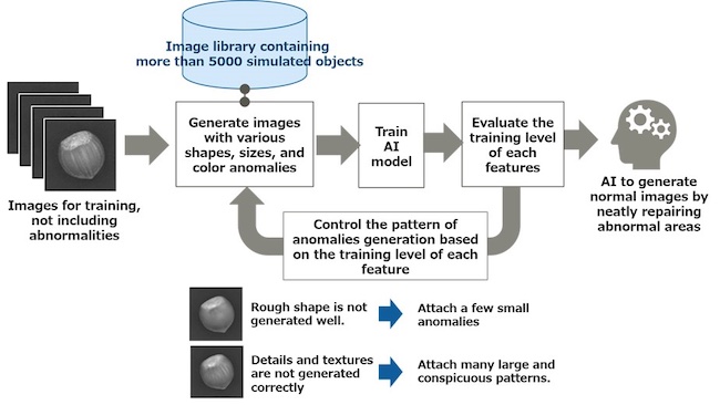
Fujitsu Laboratories announced the successful development of an AI technology for image inspection that enables highly precise detection of a wide variety of external abnormalities on manufactured goods, including scratches and production errors. The technology leverages an AI model trained on images of products with simulated abnormalities, without having to prepare training data that uses actual images of defective products pulled from the inspection process of a production line.
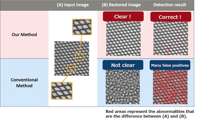
This technology is capable of correctly detecting abnormalities like frayed threads and defective wiring patterns in products that vary individually, even if they appear normal, such as carpets with different wool or color, or printed circuit boards with different wiring shapes depending on the part. The developed technology successfully achieved world leading accuracy (1) in a benchmark using public data (2) collected from external images of various manufactured goods.
Recommended AI News: Retarus and MicroCorp Announce Strategic Partnership
Fujitsu verified the effectiveness of this technology during the inspection process at the Nagano Plant of Fujitsu Interconnect Technologies Limited, a factory that manufactures electronic equipment, and confirmed its effectiveness in reducing man-hours required for inspecting printed circuit boards by 25%. The technology ultimately offers the potential to help reduce the workload of workers at manufacturing plants and improve productivity, while helping to introduce new working styles for frontline staff.
Recommended AI News: HCL Technologies launches Digital Acceleration Center in Canada
Background & Challenges
At the site of the inspection process, the inspector determines whether the product is defective based on features such as its approximate shape, detailed structure, and texture. For example, approximate shape is considered important in a shape distortion test, and texture is considered important in a condition or pattern test. Furthermore, even if the product appears normal, if there are individual variations in elements like coating, color, and wiring shape, these characteristics are examined for each item, and the inspection is conducted while distinguishing whether individual differences or abnormalities fall within the acceptable range. Therefore, when training AI to conduct quality control tasks, it is necessary to be able to capture a wide variety of features that occur on an individual basis in a normal image. However, the typical method of training an AI model using weighted and summed indices for each characteristic has led to a tendency to focus on only one characteristic, and it has proven difficult to create a model that fully grasps all the characteristics.
Recommended AI News: Cognex Presents the Edge Intelligence Platform


Comments are closed.